Here, We provide Digital Fundamentals GTU Paper Solution Winter 2024. Read the Full DF gtu paper solution given below.
DF GTU Old Paper Winter 2024 [Marks : 70] : Click Here
(a) Perform the following mathematical operations using 2’s complement method.
(i) : (9)10 + (-5)10 (ii) : (3)10 – (8)10
(i) : 2’s complement of (9)10 = 1001
2’s complement of (-5)10 = 0101
Addition : 1001 + 0101 = 1110
(9)10 + (-5)10 = 1110
(ii) : Binary of (3)10 = 0011
Binary of (8)10 = 1000
2’s complement of (8)10 = 1000
Subtraction = Binary of (3)10 + 2’s complement of (8)10
= 0011 + 1000 = 1011
(3)10 – (8)10 = 1011
(b) State and prove De-Morgan’s theorems using truth-tables.
1. Law 1 : This law states that the complement of a sum of variables is equal to the product of their individual complements.
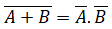
Truth table :
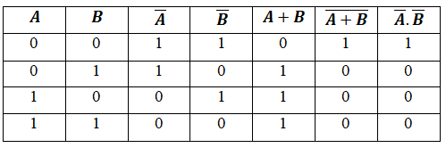
Hence, Law 1 is proved from the above truth table.
2. Law 2 : This law states that the complement of a product of variables is equal to the sum of their individual complements.
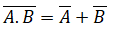
Truth table :
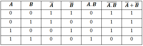
Hence, Law 2 is proved from the above truth table.
(c) Explain the characteristics of Digital ICs.
- Speed of Operation : The speed of a digital circuit is expressed in terms of propagation delay specified in nano seconds (ns). The two propagation delay times are defined as follows :
tPLH : It is the propagation delay time in going from logical LOW (0 state) to logical HIGH (1 state).
tPHL : It is the propagation delay time in going from logical HIGH (1 state) to logical LOW (0 state).
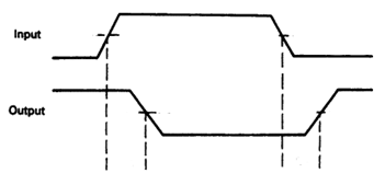
Total Propagation delay, tp = (tPLH + tPHL)/2 .
2. Power Dissipation : Any digital circuit require some power for operation that can identify using power dissipation.
ICCH: When gate is in the HIGH output the current drawn by the gate is represented by ICCH.
ICCL: When gate is in the LOW output the current drawn by the gate is represented by ICCL.
ICC(avg) = (ICCH+ICCL)/2
P = VCC*IOC = VCC*(ICCH+ICCL)/2 (mW)
3. Figure of merit : It is defined as the product of speed and power.
Figure of merit() = propagation delay(mW) * power(ns)
= 10-3 W * 10-9 s = 10-12 joules = pico joules
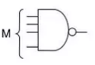
4. Fan-in : It is defined as number of input that can be connected to a gate. Gate with large fan-in are bigger and slower.
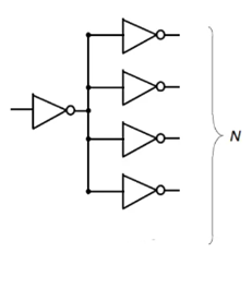
5. Fan-Out : It is the maximum number similar logic gates that a gate can drive without any degrading into voltage levels.
6. Voltage parameters :

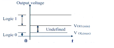
- VIH (min) : high-level input voltage, This is the minimum value of the input voltage which will be considered as a logic (HIGH) 1 level.
- VIL (max) : low-level input voltage, This is the maximum value of the input voltage which will be considered as a logic (LOW) 0 level.
- VOH (min) : high-level output voltage, This is the minimum value of the output voltage which will be considered as a logic (HIGH) 1 level.
- VOL (max) : low-level output voltage, This is the maximum value of the output voltage which will be considered as a logic (LOW) 0 level.
7. Noise Immunity : It is defined as ability of a logic circuit to tolerate the noise without causing any unwanted changes in the output. A quantitative measure of noise immunity is called as noise margin.
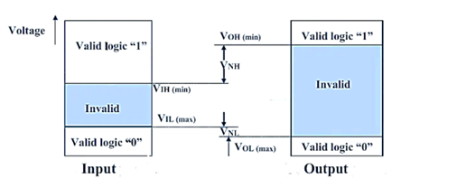
- The difference between VOH (min) and VIH (min) is known as the high level noise margin VNH. Similarly the difference between VIL (max) and VOL (max) is called as the low level noise margin VNL.
- High level noise margin, VNH = VOH (min) – VIH (min)
- Low level noise margin, VNL = VIL (max) – VOL (max)
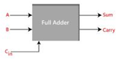
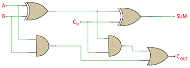
(a) Design a Full adder circuit using basic logic gates.
The half adder is used to add only two numbers. To overcome this problem, the full adder was developed. The full adder is used to add three 1-bit binary numbers A, B, and carry C. The full adder has three input states and two output states i.e., sum and carry.
Block diagram :
Truth table :
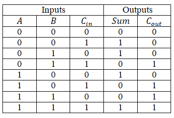
In the above table,
1. ‘A’ and’ B’ are the input variables. These variables represent the two significant bits which are going to be added.
2. ‘ Cin‘ is the third input which represents the carry. From the previous lower significant position, the carry bit is fetched.
3. The ‘Sum’ and ‘Carry’ are the output variables that define the output values.
4. The eight rows under the input variable designate all possible combinations of 0 and 1 that can occur in these variables.
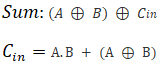
The full adder logic circuit can be constructed using the ‘AND’ and the ‘XOR’ gate with an OR gate.
(b) Design a modulo-6 ripple counter using T- flip flops.
A binary ripple counter consists of a series connection of complementing flip‐flops, with the output of each flip‐flop connected to the clock input of the next higher order flip‐flop.
- The flip‐flop holding the least significant bit receives the incoming count pulses.
- The count starts with binary 0 and increments by 1 with each count pulse input.
Step 1 : Determine the number of flip flop by 2n >> N where n: number of flip-flop and N: number of states 2n >> N = 23 >> N : n=3 flip-flops
Step 2 : Identify type of flip-flop : T flip-flop
Step 3 : Draw the truth table :
State diagram :

Step 4 : Identify Boolean expression using K-map :
Step 5 : Draw the logic circuit :
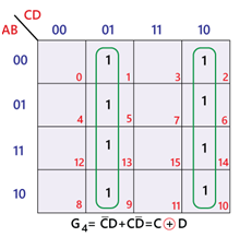
(c) Design a 4-bit binary to Gray code converter using K-map.
The Binary to Gray code converter is a logical circuit that is used to convert the binary code into its equivalent Gray code.
The 4-bit binary to gray code conversion table is as follows :
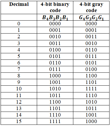
The bits of 4-bit gray code are considered as G4G3G2G1. Now from conversion table,
G4 = Σm(8,9,10,11,12,13,14,15)
G3 = Σm(4,5,6,7,8,9,10,11)
G2 = Σm(2,3,4,5,10,11,12,13)
G1 = Σm(1,2,5,6,9,10,13,14)
For G4 :
For G3 :
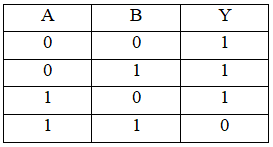
(c) Draw a two input TTL NAND gate and explain its operations.
The below diagram is the circuit diagram of a TTL NAND gate.
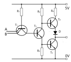
The transistor T2 has two emitters to allow two inputs into the transistor.
Now, as connected the base voltage will be at 5V. If both inputs are logic 1 (usually means about 5V too), the potential difference across base and emitter would be zero or nearly. Hence, no current will flow and the transistor is turned off.
So, the collector voltage would also be equal to about 5V. Hence, this potential can drive current through the emitter of the transistor T2. This then will allow the collector voltage of the transistor T2 to fall.
Now due to the current flowing through the emitter, there would be a voltage drop across the resistor R3. The desired voltage drop would be about 0.7V. As seen, this is the input of the transistor T3. Hence, the transistor is turned on. Due to saturation, the collector voltage will fall to about 0.2V which is a logic 0.
For the transistor T4, observe that the emitter voltage is made up of the entire voltage of the transistor T3 plus the voltage drop across the diode D about 0.7V. Hence the emitter potential would be 0.7 + 0.2 = 0.9V.
The base voltage of the transistor T4, would be the voltage across the base-emitter of T3 and the voltage of the entire transistor (i.e.) voltage across emitter-collector. This would also be equal to about 0.9V.
Hence the emitter voltage and the collector voltage are equal. So the transistor T4 will be turned off too. So the output is zero when both inputs are 1.
Truth table of NAND gate :
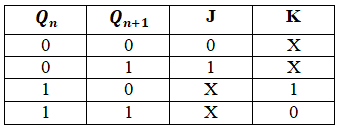
(a) Explain Race Around Condition in JK flip-flop.
For J-K flip-flop, if J=K=1, and if clock=1 for a long period of time, then Q output will toggle as long as CLK is high, which makes the output of the flip-flop unstable or uncertain.
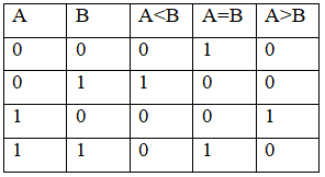
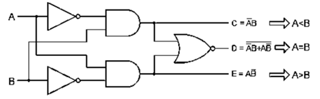
(b) Design a 1-bit Magnitude Comparator.
A comparator used to compare two bits is called a single-bit comparator.
The truth table for a 1-bit comparator is given below :
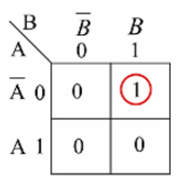
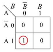
K-map for all three output :
A<B : A’B
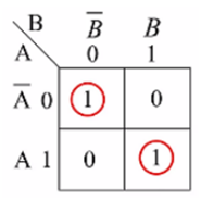
A = B : A’B’ + AB
A > B : AB’
From the above truth table logical expressions for each output can be expressed as follows : A<B : A’B, A = B : A’B’ + AB, A > B : AB’
Logic diagram for 1 Bit Comparator :
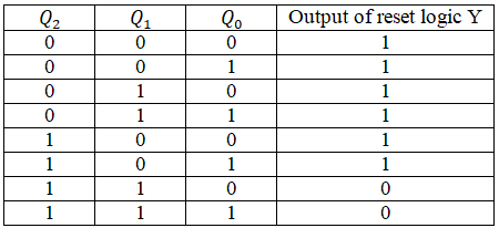
(c) Explain Hamming codes for error correction with a suitable example.
Hamming code is a set of error-correction codes that can be used to detect and correct the errors that can occur when the data is moved or stored from the sender to the receiver.
Solve Problem : Data bits 1011 must be transmitted. Construct the even parity, seven bit Hamming code for this data :

P1 checks for even parity of bit positions 1,3,5 and 7. For even parity P1 must be 1

P2 checks for even parity of bit positions 1,3,5 and 7. For even parity P2 must be 0

P3 checks for even parity of bit positions 1,3,5 and 7. For even parity P3 must be 1

There for the final code 1010101 will be transmitted.
Decode the message assuming that at most a single error occurred in each code word
Answer : message is 1000101
Bit 1,3,5,7 (1101) : error : C1=1
Bit 2,3,6,7 (0101) : No error : C2=0
Bit 4,5,6,7 (1000) : error : C3=1
The error word is C3C2C1 = 101 = (5)10, so complement the 5th bit from right .
There for the correct answer is 1010101.
(a) Find expression for the following and implement using logic gates.
F(A,B,C,D) = πM (0,2,3,6,7,8,9,12,13)
There are 3 pairs formed in the above K-map :
Pair 1 : (2,3,6,7) Pair 2 : (8,9,12,13) Pair 3 : (0,8)
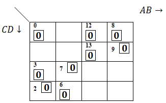
The Boolean expressions of the pairs are :
Pair 1 : A’C Pair 2 : AC’ Pair 3 : B’C’D’
F(A,B,C,D) = A’C + AC’ + B’C’D’
(b) Implement D flip-flop using JK flip-flop.
Step 1 : Identify available and required flip-flop :
Available flip-flop : JK flip-flop Required flip-flop : D flip-flop
Step 2 : Make characteristic table for required flip-flop :
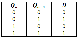
Step 3 : Make excitation table for available flip-flop :
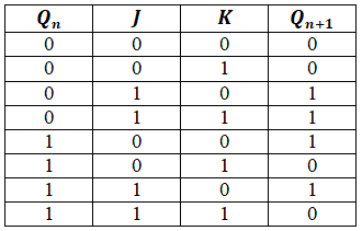
Step 4 : Write Boolean expression for available flip-flop :
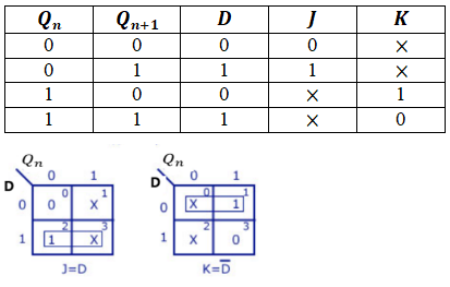
Step 5 : Draw the logic circuit :
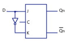
(c) Design a 4-bit twisted Ring Counter using JK flip flops.
The counter in which the output of the last flip-flop is connected to the input of the first flip-flop is called ring counter.
Number of bits required = Number of flip-flops used
So, for designing a 4-bit Ring counter we need 4 flip-flops.
In this diagram, we can see that the clock pulse (CLK) is applied to all the flip-flops simultaneously. Therefore, it is a Synchronous Counter.
Possible state : n-bit = 4
Unstable state : 2n-n = 24-4 = 16-4 = 12
(a) Differentiate Synchronous Counters and Asynchronous Counters.
| Asynchronous Counters | Synchronous Counters |
| A flip-flops are connected in such a way that the output of flip flop drives the clock of next flip-flop. | There is no connection between output of first flip flop and clock of next flip flop. |
| In asynchronous counter, circuit is simple. | In synchronous counter, circuit is complex. |
| In asynchronous counter, speed is slow. | In synchronous counter, speed is high. |
| It is slower than synchronous counters. | It is faster than asynchronous counters. |
| In asynchronous counter, there is high propagation delay. | In synchronous counter, propagation delay is less. |
| Examples : Ripple UP Counter, Ripple DOWN Counter. | Examples : Ring Counter, Johnson Counter |
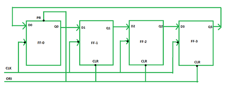
(b) Implement the following using 8:1 MUX.
F = f(A,B,C,D) = Σm(2, 4, 5, 7, 10, 14)
D0 D1 D2 D3 D4 D5 D6 D7
A’ 0 1 2 3 4 5 6 7
A 8 9 10 11 12 13 14 15
Answer : 0 0 1 0 A’ 0 A A’
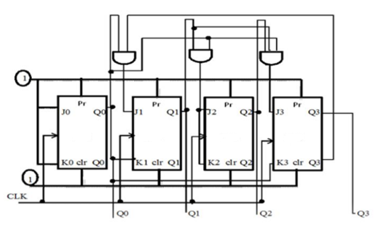
(c) Design a synchronous BCD counter using J-K flip-flops.
Step 1 : Find required number of flip flops :
Number of state : 10 Number of flip flop : 4 (2n>>N)
Step 2 : Draw state diagram :

Step 3 : Select flip flop and draw excitation table :
JK flip flop (given) Excitation table of JK flip flop :
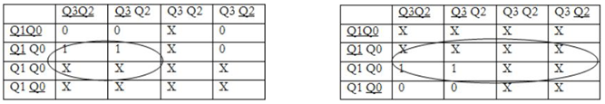
Step 4 : Find minimal expression for excitation table of flip flop :
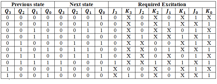
K-map :
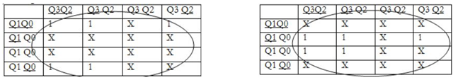
J0 = 1 K0 = 1
J1 = Q0Q3 K1 = Q0
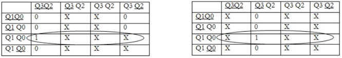
J2 = Q0Q1 K2 = Q0Q1
J3 = Q0Q1Q2 K3 = Q0
Step 5 : Draw the logic circuit :
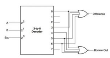
(a) Implement full subtractor using 3:8 decoder and write a truth table.
The designing of a full subtractor using 3-8 decoders can be done using active low outputs. The decoder includes three inputs in 3-8 decoders. Based on the truth table, we can write the minterms for the outputs of difference & borrow.
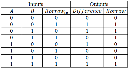
From the above truth table,
For the different functions in the truth table, the minterms can be written as 1,2,4,7, and similarly, for the borrow, the minterms can be written as 1,2,3,7. The 3-8 decoders include three inputs as well as 8 outputs like 0 to 7 numbers.
If the input of the subtractor is 000, then output ‘0’ will be active and if the input is 001, then the output ‘1’ will be active.
Now the outputs of the subtractor can be taken from 1, 2, 4 &7 to connect it to a NAND gate, then the output will be the difference. These outputs can be connected to other NAND logic gates where the output changes to the borrow.
For example, if the input is 001, then the output will be 1 that means it is active. So the output is active low and the output can be obtained from NAND gate called difference function like high and borrow function also changes out to be high. Therefore we get the preferred output. So finally, the decoder works like a full subtractor.
(b) Explain the specifications of Digital to Analog Converters.
(1) Resolution : This is defined as the smallest possible change in the analog output as a result of a change in digital input. This is also referred as step-size.
The resolution is always equal to the weight of LSB (Least Significant Bit).
- Number of possible steps or level : 2n-1
- Step size (Resolution) = Full Scale Output/ Number of steps
- % Resolution = (Step size/Full Scale output)×100 = (1/2n-1)×100
(2) Accuracy : It is a measure of the difference between the actual output voltage and the expected output voltage. I t is specified as a full scale or maximum output voltage.
(3) Setting time : Time required for DAC output to go from zero to full scale. The operating speed of DAC is specified by setting time.
(4) Offset : It is the difference between the actual output and ideal output when the digital input is zero.
(c) Explain Successive Approximation type D/A converter.
The successive approximation converter is one of the most widely used types of ADC.
- It has much shorter conversion time than the other types, with the exception of parallel type.
- It also has fixed conversion time which is not dependent on the value of the analog input.

- Figure consists of DAC, an output register, a comparator and control logic.
- The basic operations is as follows : The bits of DAC are enabled one at a time, starting with the MSB.
- As each is enabled, the comparator produces an output that indicates whether the analog input voltage is greater than or less than the output of the DAC.
- If the D/A is output is greater than analog input, the comparator output is LOW, causing the bit in control register to reset.
- If the D/A is output is greater than analog input, the comparator output is HIGH, and the bit is retained in control register.
- The system enables the MSB first, then the next significant bit, and so on.
- After all the bits of DAC have been tried, the conversion cycle is complete.
Example : Let us assume that the output of the DAC ranges from 0V to 15V as its binary input ranges from 0000 to 1111, with 0000 producing 0V and 0001 producing 1V, and so on.
- Suppose that the unknown analog input voltage VA is 10.3 V.
- On the first clock pulse, the output register is loaded with 1000, which is converted by the DAC to 8V.
- The voltage comparator determines that 8V is less than the analog input (10.3V); so, the control logic retains that bit.
- On the next clock pulse, the control circuitry causes the output register to be loaded with 1100.
- The output of the DAC is now 12V, which the comparator determines as greater than the analog input.
- Therefore, the comparator output goes LOW. The control logic clears that bit; so, the output goes back to 1000.
- On the next clock pulse, the control circuitry causes the output register to be loaded with1010.
- The output of the DAC is now 10V, which the comparator determines as less than the analog input.Thus, on the next clock pulse, the control logic causes the output register to be loaded with 1011.
- The output of the DAC is now 11V, which the comparator determines as greater than the analog input; so, the control logic clears that bit.
- Now the output is 1010 which is the nearest integer value to the input (10.3V).
- At this point, all of the register bits have been processed, the conversion is complete and the control logic activates its EOC output to signal that the digital equivalent of is now in the output register.
(a) Differentiate Static RAM and Dynamic RAM.
| Static RAM | Dynamic RAM |
| Constructed of circuits similar to D flip-flop. | Constructed of tiny capacitors that leak electricity. |
| It stores information as long as the power is supplied. | It stores information as long as the power is supplied or a few milliseconds when the power is switched off. |
| It is expensive. | It is inexpensive. |
| It cannot store many bits per chip. | It can store many bits per chip. |
| It uses more power. | It uses less power. |
| It is used for cache. | It is used for main memory. |
(b) Write a short note on FPGA.
The word field in the name refers to the ability of the gate arrays to be programmed for a specific function by the user instead of by the manufacturer of the device.
- The word array is used to indicate a series of columns and rows of gates that can be programmed by the end user.
- As compared to standard gate arrays, the field programmable gate arrays are larger devices.
- The basic cell structure for FPGA is somewhat complicated than the basic cell structure of standard gate array. The programmable logic blocks of FPGAs are called logic blocks or Configurable Logic Blocks (CLBs).
- The basic architecture of FPGA consists of an array of logic blocks with programmable row and column interconnecting channels surrounded by programmable I/O blocks as shown in figure.
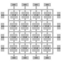
Each logic block in a generic FPGA contains several logic elements, as shown in Figure.
- Generally there can be well over ten thousand logic elements in a single chip. The Logic Element:
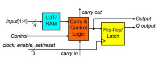
- A simplified diagram of a typical FPGA logic clement is shown in Figure.
- It contains an LUT, associated logic, and a flip-flop.
- Each logic element contains a 4-input LUT that can be programmed as logic function generator.
- It can be used to produce SOP functions or logic functions such as adders and comparators.
- When configured as an adder, the carry in and carry out allow for adder expansion.
- Using the cascade logic, an LUT can be expanded by cascading with LUT’s in other logic elements.
- The programmable selects let you choose either combinational functions from the LUT output or registered functions from the flip-flop output.
FPGA Logic Element :
(c) Explain the operation of Dual-slope A/D converter.
A dual-slope A/D converter is one of the slowest converters =, but is relatively inexpensive because it does not require precision components such as DAC.
- Because of its large conversion time, it is not used in any data acquisition application.
- The major applications are in digital voltmeters, multimeters, etc.
- Since it is not fast enough, its use is restricted to signals having low to medium frequencies.
- It uses an operational amplifier to integrate the analog input.
- The output of the integrator is a ramp, whose slope is proportional to the input signal , since the components R and C are fixed.
- If the ramp is allowed to continue for a fixed time, the voltage it reaches in that time, depends on the slope of the ramp and, therefore, on the value of Ein.

- The basic principles of me integrating ADC is that, the voltage reached by the ramp controls the length of time that the binary counter is allowed to count.
- Thus, a binary number proportional to the value of Ein is obtained.
- In the dual-slope ADC, two integrations are performed.
- Figure shows the functional block diagram of a dual-slope ADC.
- Assume that the counter is reset and the output of the integrator is zero.
- A conversion begins with the switch connected to the analog input.
- Assume that the input is a negative voltage and is constant for a period of time; so, the output of the integrator is a positive ramp.
- The ramp is allowed to continue for a fixed time and the voltage it reaches in that time is directly dependent on the analog input.
- The fixed time is controlled by sensing the time when the counter reaches a particular count.
- At that time, the counter is reset and the control circuitry causes the switch to be connected to a reference voltage EREF, having a polarity opposite to that of the analog input; in this case a positive reference voltage.
- Therefore, the output of the integrator is a negative going ramp, beginning from the positive value it reached during the first integration.
- The AND gate is enabled and the counter starts counting.
- When the ramp reaches 0V, the voltage comparator switches to LOW, inhibiting the clock pulses and the counter stops counting.
- The binary count is latched, thus, completing one conversion.
- The count it contains at that time is proportional to the time required for the negative ramp to reach zero, which is proportional to the positive voltage reached during the first integration, which in turn is proportional to the analog input.
- The accuracy of the converter does not depend on the values of the integrator components or upon any changes in them.
- The accuracy does depend on EREF; so, the reference voltage should be very precise.
(a) Explain basic structure of a CCD (Charge Coupled Device).
Charge-coupled device memory is a type of dynamic memory in which packets of charge are continuously transferred from one MOS device to another. The structure of a MOS charge-coupled device is quite simple, as shown in the figure. It consists simply of a P substrate, an insulating oxide layer, and isolated gates.
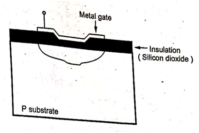
- When a high voltage is applied to the metal gate, holes are repelled from a region beneath the gate in the P-type substrate. This region, called a potential well, is then capable of accepting a packet of negative charged electrons. Therefore, data is stored in a CCD as charge, and it is transferred from one device to an adjacent one by clocking their gates.
- The charge-coupled devices are built as a serial-in, serial-out MOS shift registers, each shift register being a line of charge-coupled devices. By controlling the timing of the clock signals applied to the shift registers, data can be accessed one bit at a time from a single register or several bits at a time form multiple registers.
- The main advantage of CCD is that its simple cell structure. It makes it possible to construct large-capacity memories at low cost. Since CCDs are dynamic in nature, they must be periodically refreshed, and must be driven by rather complex, multi phase clock signals.
- Another disadvantages of CCDs is due to serial data storage. Serial data storage has a longer access times in comparison to semiconductor RAM memory.
- CCDs can be used for digital or analog delay, and as serial data memories. Another exciting application of CCDs is as the light sensitive image sensor in television cameras.
(b) Write a short note on Programmable Array Logic.
PAL is a programmable logic device that has Programmable AND array & fixed OR array. The advantage of PAL is that we can generate only the required product terms of Boolean function instead of generating all the min terms by using programmable AND gates. The block diagram of PAL is shown in the following figure.
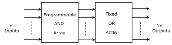
- Here, the inputs of AND gates are programmable. That means each AND gate has both normal and complemented inputs of variables. So, based on the requirement, we can program any of those inputs. So, we can generate only the required product terms by using these AND gates.
- Here, the inputs of OR gates are not of programmable type. So, the number of inputs to each OR gate will be of fixed type. Hence, apply those required product terms to each OR gate as inputs. Therefore, the outputs of PAL will be in the form of sum of products form.
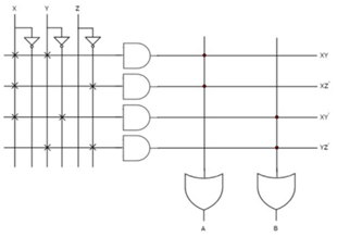
- EXAMPLE : Implement the following Boolean functions using PAL. A=XY+XZ′ B=XY′+YZ′
SOLUTION : The given two functions are in sum of products form. There are two product terms present in each Boolean function. So, we require four programmable AND gates & two fixed OR gates for producing those two functions. The corresponding PAL is shown in the following figure.
(c) Explain various types of Read Only Memory.
1.Masked Read Only Memory (MROM) :It is the oldest type of read only memory (ROM). It is a hardware memory device in which programs and instructions are stored at the time of manufacturing by the manufacturer.
- So it is programmed during the manufacturing process and can’t be modified, reprogrammed, or erased later.
- It is the very first ROM in hard-wire devices. Masked ROMs consist of pre-planned programs of data, otherwise instructions and it is cheaper as well.
2.Programmable Read Only Memory (PROM) : PROM is a blank version of ROM.
- It is manufactured as blank memory and programmed after manufacturing.
- We can say that it is kept blank at the time of manufacturing.
- You can purchase and then program it once using a special tool called a programmer.
- To write data onto a PROM chip; a device called PROM programmer or PROM burner is used. The process or programming a PROM is known as burning the PROM. Once it is programmed, the data cannot be modified later, so it is also called as one-time programmable device.
- Uses: It is used in cell phones, video game consoles, medical devices, RFID tags, and more.
3.Erasable Programmable Read Only Memory (EPROM) :
- EPROM is a type of ROM that can be reprogrammed and erased many times. The method to erase the data is very different; it comes with a quartz window through which a specific frequency of ultraviolet light is passed for around 40 minutes to erase the data.
- So, it retains its content until it is exposed to the ultraviolet light. You need a special device called a PROM programmer or PROM burner to reprogram the EPROM.
Uses: It is used in some micro-controllers to store program, for program development, as BIOS chip in computers, as program storage chip in modem, video card and many electronic gadgets.
4.Electrically Erasable and Programmable Read Only Memory (EEPROM) :
- ROM is a type of read only memory that can be erased and reprogrammed repeatedly, up to 10000 times.
- It is also known as Flash EEPROM as it is similar to flash memory. It is erased and reprogrammed electrically without using ultraviolet light.
- Access time is between 45 and 200 nanoseconds.
- The data in this memory is written or erased one byte at a time; byte per byte, whereas, in flash memory data is written and erased in blocks.
- So, it is faster than EEPROM. It is used for storing a small amount of data in computer and electronic systems and devices such as circuit boards.
Uses: The BIOS of a computer is stored in this memory.
5.FLASH ROM :
- It is an advanced version of EEPROM. It stores information in an arrangement or array of memory cells made from floating-gate transistors.
- The advantage of using this memory is that you can delete or write blocks of data around 512 bytes at a particular time.
- Whereas, in EEPROM, you can delete or write only 1 byte of data at a time. So, this memory is faster than EEPROM.
- It can be reprogrammed without removing it from the computer. Its access time is very high, around 45 to 90 nanoseconds. It is also highly durable as it can bear high temperature and intense pressure.