Here In this blog, We provide Physics-II GTU paper solution winter 2021. Read the Full Physics-II gtu paper solution given below.
Physics - II GTU Old Paper Winter 2021 [Marks : 70] : Click Here
(a) Define absorption, spontaneous emission and stimulated emission for
bulk semiconductors.
Absorption: The process by which photons are absorbed by the electrons in a bulk semiconductor, leading to a transition from the valence band to the conduction band.
Spontaneous emission: The process by which an electron in an excited state spontaneously emits a photon and returns to the ground state.
Stimulated emission: The process by which an incoming photon with the correct energy causes an electron in an excited state to emit a second photon with the same energy and phase, leading to coherent amplification of the light.
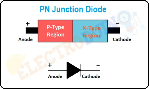
(b) Write a short note on P-N junction diode
A P-N junction diode is a two-terminal device that is commonly used as a rectifier, switch, and voltage-controlled current source.
It is made by connecting a p-type semiconductor and an n-type semiconductor, creating a p-n junction.
The p-side is positively charged and the n-side negatively charged. When a voltage is applied, current can flow in one direction (forward bias) but is blocked in the opposite direction (reverse bias), making the P-N junction diode a one-way electrical valve.
The P-N junction diode is widely used in electronic circuits for power conversion, signal processing, and light detection.
(c) Give assumptions of classical free electron theory and discuss its
limitations
Assumptions of classical free electron theory:
- Electrons in a metal are considered to be free and are not bound to any specific lattice site.
- The electrons in a metal occupy an energy band known as the conduction band.
- The electrons in a metal are treated as a gas of non-interacting particles.
- The electrons are in thermal equilibrium with the lattice and their distribution follows the Fermi-Dirac statistics.
Limitations:
- The theory does not consider the interactions between electrons and lattice vibrations (phonons), which can have a significant effect on the electrical and thermal properties of metals.
- The theory assumes that the electrons are completely free, but in reality, they are subject to various interactions and scattering mechanisms, such as impurities and defects, that affect their mobility and resistance.
- The theory does not take into account the quantum mechanical nature of the electrons and the effects of quantization, such as the formation of energy bands.
- The theory does not account for the influence of the electron-electron interactions on the electrical properties of metals, which can be important in certain cases.
(a) Find the temperature at which there is 1% probability that a state with
energy 2eV is occupied. Given that Fermi energy is 1.5 eV.
energy : 0.5 eV
Probability, f(E)= 1% = 1/100
E – EF = 0.5 eV
T = ?
F(E) = 1/ (1 + exp(E – E(F))/K(b)T
K(B) =1.381 × 10⁻²³J/K
=1.381 × 10⁻²³ × 6.24 × 10¹⁸ eV/K
Substituting the value we get:
1/100 = 1/ 1 + exp[0.5/(861.744 × 10⁻5T)]
100 = 1 + exp[5801.87/T]
100 ≈ exp[ 5801.87/T]
Taking In on both sides, we get:
Ln 100 = 5801.87/ T
T = 5801.87 / 4.605 = 1259.98 K
(b) What is drift and diffusion current in p-n junction diode?
Drift current: The drift current in a p-n junction diode is the movement of charged carriers (electrons and holes) under the influence of an electric field.
This current is proportional to the electric field and is responsible for the flow of current when the diode is forward-biased.
Diffusion current: The diffusion current in a p-n junction diode is the result of the concentration gradient of charge carriers, which leads to a net flow of carriers from high to low concentration regions.
This current is independent of the electric field and is responsible for the flow of current when the diode is reverse-biased. The diffusion current is proportional to the difference between the concentration of holes and electrons on either side of the p-n junction.
(c) Explain the Kronig-Penny model of solids and show that how it
explains the origin of band gap in solids.
Kronig Penny Model
The Kronig-Penny model of solids is a simple model that explains the formation of energy bands in solids.
The model assumes that a solid is made up of a periodic array of identical atoms, each of which contributes one electron to the conduction band. The electrons in the conduction band can be thought of as plane waves that interact with each other, creating a band structure.
In the Kronig-Penny model, the energy bands are created by the interaction between the electrons in the conduction band and the periodic potential of the lattice.
The periodic potential acts as a series of barriers and wells that the electrons must overcome. The electrons with low energy are confined to the wells, while those with higher energy can overcome the barriers and occupy the conduction band.
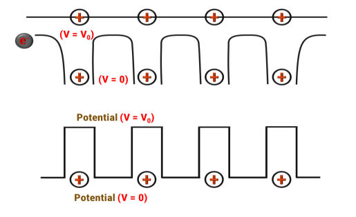
The band gap in a solid is the energy difference between the top of the valence band and the bottom of the conduction band. The origin of the band gap can be explained by the Kronig-Penny model as follows: the interaction between the electrons in the conduction band and the periodic potential of the lattice creates a finite width of the conduction band, which results in a gap between the top of the valence band and the bottom of the conduction band. The size of the band gap is determined by the height and width of the potential barriers, and the interactions between the electrons.
[OR] (c) Explain intrinsic and extrinsic (N & P type) semiconductors with the
help of energy band diagram.
Intrinsic Semiconductors:
Intrinsic semiconductors are pure, undoped semiconductors that have equal numbers of electrons and holes.
In an intrinsic semiconductor, the conduction band and valence band are separated by a band gap, which determines the energy required to excite an electron from the valence band to the conduction band.
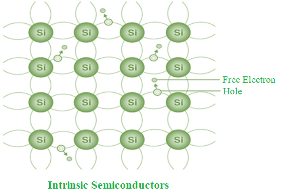
In this diagram, the valence band is fully occupied, and the conduction band is empty. The band gap is the energy required to excite an electron from the valence band to the conduction band.
Extrinsic Semiconductors:
Extrinsic semiconductors are doped semiconductors, meaning they have been intentionally contaminated with impurities that provide extra electrons or holes.
Extrinsic semiconductors can be either n-type or p-type.
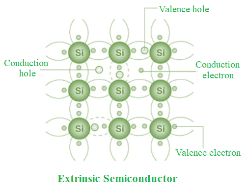
- N-type Semiconductors:
N-type semiconductors are doped with impurities that have one more electron in their valence band than the semiconductor. In an n-type semiconductor, the extra electrons occupy the conduction band, leaving holes in the valence band.
- P-type Semiconductors:
P-type semiconductors are doped with impurities that have one fewer electron in their valence band than the semiconductor. In a p-type semiconductor, the missing electrons create holes in the valence band that can be filled by electrons from the conduction band.
(a) In an N-type semiconductor, the Fermi level lies 0.3 eV below the
conduction band at room temperature. If the temperature is increased to
330K, Find the position of Fermi level.
When the temperature of a semiconductor is raised to KT, the position of Fermi level is raised by KT (kT is the amount of heat required to increase the thermodynamic entropy of a system by k) from its initial position at a given temperature, where ‘K’ is Boltzmann constant
(K = 1.38× 10⁻²³JK−1).
Also,
Eg(energy band gap) ∝ 1/T
Eg/E’g=T’/T
0.3/E’g=330/300
E’g=300×0.3/330
=0.27eV
0.27 eV below the conduction band.
(b) Write an expression for Fermi Dirac distribution function f(E). Show
that at all temperatures (T > 0K) probability of occupancy of Fermi
level is 50%.
// Please provide the answer if you know.
(c) Discuss the effect of temperature on the Fermi level in extrinsic (N & P
type) semiconductors.
OR
(a) Find the concentration of holes and electrons in N-type silicon if the
conductivity is 0.1 -cm-1, mobility of electrons is 1300 cm2/V-s and total carrier concentration is 1.5×10¹⁰ carriers / cm3.
Please provide the answer if you know.
(b) Establish the relation between Einstein’s coefficients.
Please provide the answer if you know.
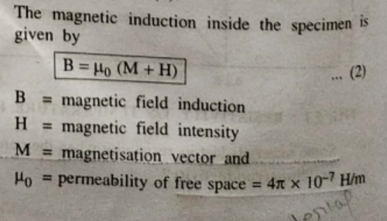
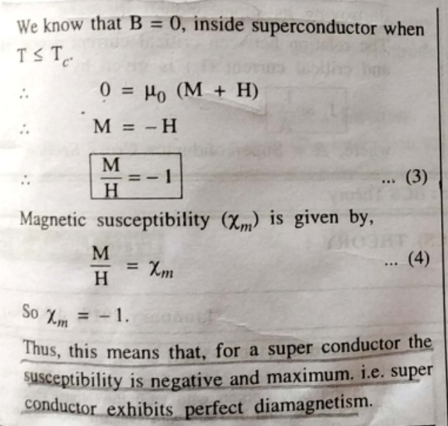
(c) Explain Meissener’s effect in detail and show that for superconductor,
χm = –1.
When superconductor is placed in an external magnetic field, it expels all magnetic flux lines from it. This is known as “Meissner effect”.
When the superconducting material is placed in a magnetic field (H> Hc) at room temperature, the magnetic field is found to penetrate normally throughout the material it shown in (a).
However, if the temperature is lowered below T and with H<Hc the material is found to reject all the magnetic field penetrating through it shown in (b).

(a) Write a short note on effective mass of electron.
The effective mass of an electron in a solid is a measure of the electron’s effective mass relative to the free electron mass.
In a solid, electrons are subject to various interactions with lattice vibrations and other electrons, which affects their motion. The effective mass of an electron takes into account these interactions and provides a more accurate representation of the electron’s behavior in a solid than the free electron mass.
The effective mass is different for electrons in different bands and can be either larger or smaller than the free electron mass.
In general, electrons in the conduction band have a smaller effective mass than the free electron mass, which makes them more mobile and contributes to the electrical conductivity of a material. On the other hand, electrons in the valence band have a larger effective mass, which makes them less mobile and contributes to the material’s insulating properties.
(b) What is mass action law? Explain Schottky junction.
Mass Action Law:
The Mass Action Law is a chemical principle that relates the rate of a chemical reaction to the concentration of reactants. According to the law, the rate of a reaction is proportional to the product of the concentrations of the reactants raised to their stoichiometric coefficients.
The equation for the Mass Action Law is given by:
rate = k [A]x [B]y
where k is the rate constant, [A] and [B] are the concentrations of the reactants A and B, x and y are the stoichiometric coefficients of A and B, and the rate is the change in concentration per unit time.
Schottky Junction:
A Schottky junction is a type of metal-semiconductor junction that is commonly used in electronic devices.
It is formed by the direct contact of a metal and a semiconductor, with no insulating layer between them.
Unlike a P-N junction, which relies on doping to create a junction, a Schottky junction is formed by the difference in work function between the metal and the semiconductor.
In a Schottky junction, electrons flow from the metal to the semiconductor, creating a depletion region in the semiconductor that acts as a barrier to the flow of electrons. The Schottky junction acts as a rectifying diode, allowing current to flow in only one direction.
This behavior makes Schottky diodes useful for various applications, including rectification, voltage clamping, and switching.
The behavior of a Schottky junction can be described by the Mass Action Law, as the rate of current flow through the junction depends on the concentration of electrons in the metal and the semiconductor and the height of the potential barrier at the junction.
(c) Explain Drude model and discuss how it is used for Hall measurements and magnetoresistance.
Drude Model:
The Drude Model is a classical model of electronic transport in metals.
According to the model, metals are composed of a large number of free electrons that are subject to random collisions with lattice vibrations and other electrons.
The model assumes that the electrons are in thermal equilibrium with the lattice, and that their motion is described by the laws of classical mechanics.
The Drude Model describes the behavior of free electrons in terms of their mobility, which is the ratio of their velocity to the applied electric field.
The model predicts that the electrical conductivity of a metal is proportional to the density of free electrons and their mobility.
The Drude Model is used to interpret Hall measurements, which are used to determine the charge carrier density and mobility in a material. In a Hall measurement, a material is subjected to a magnetic field, and the transverse voltage produced by the field is measured. The Drude Model predicts that the Hall voltage is proportional to the magnetic field and the charge carrier density and mobility.
The Drude Model is also used to understand magnetoresistance, which is the change in resistance of a material in response to a magnetic field. According to the Drude Model, magnetoresistance arises from the scattering of electrons by magnetic impurities, which affects their mobility and changes their mean free path. The Drude Model predicts that the magnetoresistance of a material is proportional to the magnetic field and the density of magnetic impurities.
OR
(a) What is an exciton? What is DLTS? Define Hall mobility
Exciton:
An exciton is a bound state of an electron and a hole in a solid, such as a semiconductor. When a photon is absorbed in a semiconductor, an electron is excited from the valence band to the conduction band, leaving behind a positively charged hole in the valence band.
DLTS:
DLTS stands for Deep Level Transient Spectroscopy. It is a technique used to study the energy levels of impurities or defects in a solid, such as a semiconductor.
Hall Mobility
The Hall mobility is a measure of the mobility of charge carriers in a material, such as a metal or a semiconductor. The Hall mobility is defined as the ratio of the transverse voltage to the magnetic field, and is a measure of the ease with which charge carriers move in response to an electric field.
(b) What is Fermi level and Fermi energy? What is Photovoltaic Cell?
Fermi Level & Fermi Energy:
The Fermi level (also known as the Fermi energy) is the highest energy occupied by electrons in a solid, such as a metal or a semiconductor, at absolute zero temperature.
At finite temperatures, the Fermi level is shifted due to thermal excitations. The Fermi level is an important parameter in the characterization of electronic materials, and is used to study their transport and optical properties, such as conductivity, resistivity, and absorption.
Photovoltaic Cell:
A photovoltaic cell, also known as a solar cell, is a device that converts light energy into electrical energy.
Photovoltaic cells are made from semiconductor materials, such as silicon, that have a bandgap large enough to absorb light and create an electric field.
When light is absorbed in a photovoltaic cell, electrons are excited from the valence band to the conduction band, creating a flow of current. Photovoltaic cells are used in solar panels and other applications where renewable energy is needed, and play an important role in reducing greenhouse gas emissions and mitigating climate change.
(c) Explain four point probe method with diagram for the measurement of resistivity of bulk sample.
The four-point probe method is technique for the measurement of the electrical resistivity of bulk samples, such as metals and semiconductors.
It consists of four electrodes, or probes, placed on the sample at fixed positions, and a current is passed between two of the probes while the voltage measure between the other two probes.
The distance between the voltage probes is typically much larger than the distance between the current probes, to reduce the effect of contact resistance.
The resistivity of the sample is then calculated from the measured voltage and current using Ohm’s law.
Diagram: A diagram of the four-point probe method can be seen as follows:
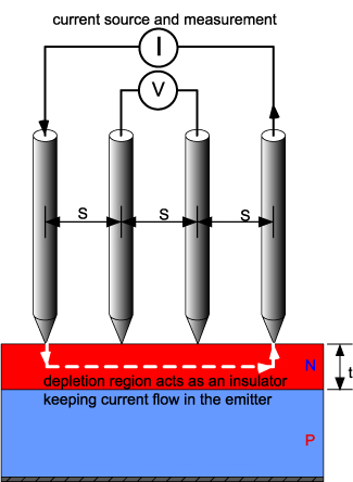
In the diagram, the current I, passes between probes 1 and 2, and the voltage V is between probes 3 and 4.
The resistivity of the sample can then be calculated as ρ = V/I, where ρ is the resistivity of the sample, V is the voltage, and I is the current.
The four-point probe method is widely used in materials science and electronic engineering to study the electrical properties of materials, including conductivity, resistivity, and mobility.
(a) Explain Fermi Golden rule for transition probability
(b) What is Josephson junction? Write a short note on SQUID.
Josephson Junction
A Josephson junction is a type of superconducting electrical junction, which consists of two superconductors separated by a thin insulating layer.
When the junction is biase with a DC voltage, a supercurrent flows through the junction, which is proportional to the sine of the phase difference between the two superconductors. The Josephson effect, which is the flow of supercurrent through the junction, is a direct consequence of the quantum mechanical properties of superconductors.
SQUID
A SQUID (Superconducting Quantum Interference Device) is a sensitive magnetic sensor that uses the Josephson effect.
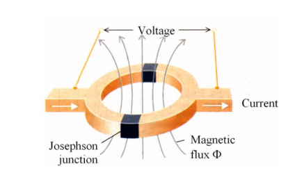
It consists of a loop of superconducting material, with two Josephson junctions in series, that acts as a quantum mechanical phase-sensitive detector.
When a magnetic field is applied to the SQUID, it modulates the phase difference between the two superconductors, leading to a change in the supercurrent through the junctions.
By measuring the supercurrent, the SQUID can detect very weak magnetic fields, making it useful in a variety of applications, including medical imaging, geophysics, and materials science.
(c) Explain how to measure band gap of the semiconductor using UV-Vis
spectroscopy.
Bandgap refers to the energy difference between bottom of conduction band and top of valence band, through which electrons are able to jump from one band to another.
The instrument used in UV-Vis spectroscopy is called UV-Vis spectro-photometer.It measure the intensity of light after passing through a sample (I), and compares it to the intensity of light before it passes through the sample (I0).
A light of wavelength (λ) and energy (hv) is made to pass through monochromator to get a parallel beam.
Transmittance (T) = I/I0
Absorption (A) = log(I/I0)
The Tauc’s relation is used to determine the bandgap (Eg) in semiconductor.
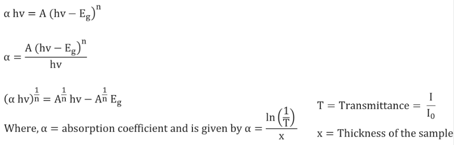
- n = 1/2, 2, 3/2, and 3 for direct allowed, indirect allowed, direct
forbidden, and indirect forbidden transitions respectively.
OR
(a) Calculate the critical current for a superconducting wire of lead having
a diameter of 1mm at 4.2 K. Critical temperature for lead is 7.18 K and
Hc(0) = 6.5 x 10⁴ A/m.
Critical current Ic = 2πrHc
Ic = 2* 3.14 * 0.5 *103 * 6.5 x 104
Ic = 134.26 A.
(c) What is superconductivity? Explain any six properties of
superconductor.
Superconductivity is a phenomenon in which a material loses all resistance to electrical current below a certain temperature, known as the critical temperature. In other words, electrical current can flow without any loss of energy.
Six properties of superconductors are:
- Zero resistance: The resistance to electrical current in a superconductor is zero, resulting in an infinite conductivity.
- Meissner Effect: A superconductor expels magnetic fields from its interior, leading to a phenomenon known as the Meissner Effect.
- Perfect diamagnetism: Due to the Meissner Effect, a superconductor is perfectly diamagnetic, meaning it repels magnetic fields.
- Energy gap: Superconductors have a characteristic energy gap in their density of states, known as the superconducting gap.
- Type-I and Type-II superconductors: Superconductors are classified into two types based on their magnetic behavior: Type-I and Type-II.
- Critical current density: The maximum current flow in a superconductor without breaking down the superconducting state is known as the critical current density.
Read More : PPS GTU Paper Solution Winter 2021
Read More : BME GTU Paper Solution Winter 2021
“Do you have the answer to any of the questions provided on our website? If so, please let us know by providing the question number and your answer in the space provided below. We appreciate your contributions to helping other students succeed.