Here, We provide Digital Fundamentals GTU Paper Solution Winter 2021. Read the Full DF gtu paper solution given below.
DF GTU Old Paper Winter 2021 [Marks : 70] : Click Here
Question: 1
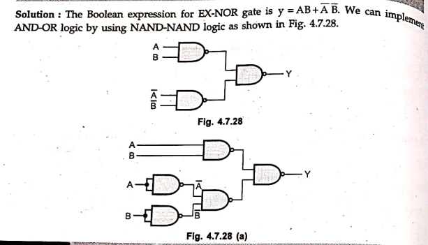
(a) Implement EX-NOR using the NAND gate.
- Block Diagram
(b) Convert the decimal number 225.225 to octal and hexadecimal.
Binary Number
- Binary conversion of 225 is (11100001)
- 0.225 in decimal is equivalent to (.0011100110011001101) in binary
- So 225.225 in binary is 11100001.0011100110011001101
Octal Number
- The equivalent octal number is
- 011 100 001.001 110 011 001 100 110 100
3 4 1 . 1 6 3 1 4 6 4
Octal number is (341.1631464)8
HexaDecimal Number
- The equivalent hexadecimal number is
- 1110 0001.0011 1001 1001 1001 1010
E 1 3 9 9 9 A
Hexadecimal number is (E1.39)16
(c) Give a classification of logic families and compare CMOS and TTL.
Logic families are mainly classified as Bipolar Logic Families and Unipolar Logic Families.
Bipolar Logic Families: It mainly uses bipolar devices like diodes, and transistors in addition to passive elements like resistors and capacitors. These are sub-classified as the saturated bipolar logic family and the unsaturated bipolar logic family.
- Saturated Bipolar Logic Family: In this family, the transistors used in ICs are driven into saturation. For example:
- Transistor-Transistor Logic (TTL)
- Resistor-Transistor Logic (RTL)
- Direct Coupled Transistor Logic (DCTL)
- Diode Transistor Logic (DTL)
- High Threshold Logic(HTL)
- Integrated Injection Logic (IIL or I 2 L)
- Unsaturated bipolar logic family: In this family, the transistors used in IC are not driven into saturation. For example:
- Schottky TTL
- Emitter Coupled Logic(ECL)
Unipolar Logic Families: It mainly uses Unipolar devices like MOSFETs in addition to passive elements like resistors and capacitors. These logic families have the advantages of high speed and lower power consumption than Bipolar families. These are classified as:
- PMOS or P-Channel MOS Logic Family
- NMOS or N-Channel MOS Logic Family
- CMOS Logic Family
- Compare CMOS and TTL
CMOS (Complementary Metal-Oxide-Semiconductor) and TTL (Transistor-Transistor Logic) are two different logic families that are commonly used in digital electronic circuits.
- Power Consumption: CMOS is known for its low power consumption, making it suitable for battery-powered and low-power applications. TTL, on the other hand, requires a significant amount of power.
- Speed: TTL is generally faster than CMOS.
- Noise Immunity: CMOS is more sensitive to noise and requires protection against static discharge, while TTL is more robust in this regard.
- Voltage Level: TTL uses a 5V power supply to represent the logical states of 0 and 1, while CMOS uses a higher voltage level (typically between 3.3V and 5V)
- Fan-out: TTL can handle more loads than CMOS.
- Temperature range: TTL can operate in a wider temperature range than CMOS.
- Production cost: CMOS is cheaper to produce than TTL.
(a) Convert F(A,B,C) = BC+A into standard minterm form.
Please provide the answer if you know.
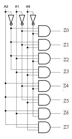
(b) With a logic diagram and truth table, explain the working of 3 lines to an 8-line decoder.
This decoder circuit gives 8 logic outputs for 3 inputs and has a enable pin. The circuit is designed with AND and NAND logic gates. It takes 3 binary inputs and activates one of the eight outputs. 3 to 8-line decoder circuit is also called a binary to an octal decoder.
Logic diagram –
Truth Table :
| A0 | A1 | A2 | E | Z0 | Z1 | Z2 | Z3 | Z4 | Z5 | Z6 | Z7 |
| x | x | x | 0 | 0 | 0 | 0 | 0 | 0 | 0 | 0 | 0 |
| 0 | 0 | 0 | 1 | 0 | 0 | 0 | 0 | 0 | 0 | 0 | 1 |
| 0 | 0 | 1 | 1 | 0 | 0 | 0 | 0 | 0 | 0 | 1 | 0 |
| 0 | 1 | 0 | 1 | 0 | 0 | 0 | 0 | 0 | 1 | 0 | 0 |
| 0 | 1 | 1 | 1 | 0 | 0 | 0 | 0 | 1 | 0 | 0 | 0 |
| 1 | 0 | 0 | 1 | 0 | 0 | 0 | 1 | 0 | 0 | 0 | 0 |
| 1 | 0 | 1 | 1 | 0 | 0 | 1 | 0 | 0 | 0 | 0 | 0 |
| 1 | 1 | 0 | 1 | 0 | 1 | 0 | 0 | 0 | 0 | 0 | 0 |
| 1 | 1 | 1 | 1 | 1 | 0 | 0 | 0 | 0 | 0 | 0 | 0 |
(c) Explain the Successive Approximation A/D converter in detail.
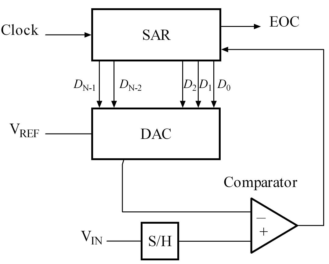
A successive approximation A/D converter is a type of analog-to-digital (A/D) converter that uses a successive approximation technique to determine the digital equivalent of an analog input voltage. The basic principle behind a successive approximation A/D converter is to compare the input voltage to a series of reference voltages and use the result of these comparisons to generate a digital output.
The successive approximation conversion process can be broken down into several main steps:
- Initialization: The process starts with the digital-to-analog converter (DAC) output set to the midpoint of the input voltage range, and the most significant bit (MSB) of the digital output is set to 1.
- Comparison: The input voltage is compared to the DAC output. If the input voltage is higher than the DAC output, the MSB of the digital output is kept as 1. If the input voltage is lower than the DAC output, the MSB is set to 0.
- Bit shifting: The comparator output is used to shift the next most significant bit (NSB) of the digital output. The NSB is set to 1 if the input voltage is higher than the DAC output, and 0 if the input voltage is lower.
- Update: The DAC output is updated based on the current state of the digital output. The DAC output is increased if the NSB is 1 and decreased if the NSB is 0.
- Repeat: The process is repeated for the next most significant bit until all digital output bits have been determined.
- Conversion: The final digital output is the digital equivalent of the input voltage.
(c) A combinational logic is defined by functions: F1(A,B,C) = ∑m (3,5,6,7) F2(A,B,C) = ∑m (0,2,4,7) Implement the circuit with PLA having 3 inputs, 4 product terms & 2 outputs.
Please provide the answer if you know.
(a) Simplify the Boolean expression: F(x,y,z) = ∑m (0,1,3,4,5,7)
Please provide the answer if you know.
(b) Explain S-R clocked flip flop.
An S-R (Set-Reset) Clocked Flip-Flop is a type of Flip-Flop that uses two inputs, S (set) and R (reset), and a clock input to control the state of the flip-flop. The flip-flop is a synchronous circuit, meaning that the state of the flip-flop changes only when a clock signal is applied.
- Block Diagram

The working of an S-R Clocked Flip-Flop can be described as follows:
When a rising edge of the clock signal is applied, the inputs S and R are latched and the state of the flip-flop is determined.
- If both S and R are at logic low, the state of the flip-flop does not change, and it remains in its previous state.
- If S is at logic high and R is at logic low, the output Q is set to logic high and the output Q’ is set to logic low. This is known as the set state.
- If S is at logic low and R is at logic high, the output Q is set to logic low and the output Q’ is set to logic high. This is known as the reset state.
- If both S and R are at logic high, the flip-flop is in an undefined state and the output is unpredictable.
(c) Design a full adder circuit using a decoder and multiplexer.
Full Adder Circuit Using 3 to 8 Decoder

Full Adder Circuit Using Multiplexer

OR
(a) Generate AND & EX-OR gates using NOR gate.
- AND gate using NOR Gate.
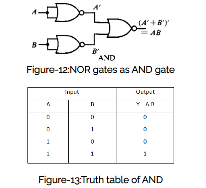
- EX-OR Gate using NOR Gate.

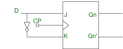
(b) Implement D flip flop using JK flip flop.
Step 1: Write a characteristic table for the required flip-flop using D-flip-flop
| D | Q | Q’ |
| 0 | 0 | 0 |
| 0 | 1 | 0 |
| 1 | 0 | 1 |
| 1 | 1 | 1 |
Step 2: We construct the characteristic table of the D flip-flop and the excitation table of the JK flip-flop.
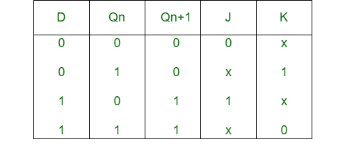
Step 3: Using the K-map we find the boolean expression of J and K in terms of D.
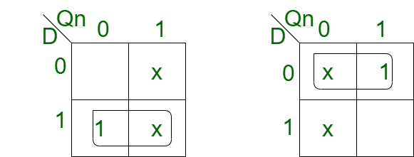
Step 4: We construct the circuit diagram of the conversion of JK flip-flop into D flip-flop.
(c) Design a counter to generate the repetitive sequence 0,4,2,1,6.
Please provide answer if you know
(a) What is the race-around condition in JK flip flop?
A race-around condition in a J-K Flip-Flop is a phenomenon that occurs when the J and K inputs change state simultaneously and both inputs are at logic level 1. In this condition, the output of the Flip-Flop will change state twice before the clock pulse ends, thus creating an unstable output. This is known as a race-around condition.
To avoid a race-around condition, it is recommended to use a pulse generator circuit that ensures that the J and K inputs are never at logic high at the same time.
(b) Construct a ring counter with five timing signals.
A ring counter is a type of shift register that generates a sequence of timing signals. To construct a ring counter with five timing signals, we can use a series of D Flip-Flops and a multiplexer. Here is an example of how it can be done:
- Use five D Flip-Flops (such as 74LS74) to form a shift register. Connect the output of each Flip-Flop to the input of the next Flip-Flop in the series.
- Connect the output of the last Flip-Flop in the series back to the input of the first Flip-Flop to create a ring.
- Connect the clock input to all Flip-Flops.
- Connect the Q output of each Flip-Flop to the input of a multiplexer (such as 74LS157)
- Connect the output of the multiplexer to the final output.
- Connect the control input of the multiplexer to a control signal that will select the output of the flip-flops.
When the clock signal is applied, the Flip-Flops will shift the state of the output, creating a sequence of timing signals. The multiplexer will select the output of the flip-flops based on the control signal, allowing to the output of the desired timing signal.
// please provide diagram for this
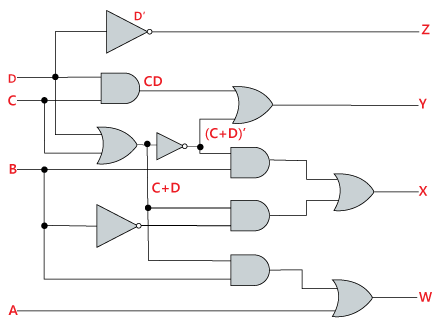
(c) Design BCD to Excess 3 code converters using a minimum number of NAND gates.
Truth Table of BCD and Excess-3 Code
| Decimal Number | BCD Code | Excess-3 Code |
| A | B | C | D | W | x | y | z | |
| 0 | 0 | 0 | 0 | 0 | 0 | 0 | 1 | 1 |
| 1 | 0 | 0 | 0 | 1 | 0 | 1 | 0 | 0 |
| 2 | 0 | 0 | 1 | 0 | 0 | 1 | 0 | 1 |
| 3 | 0 | 0 | 1 | 1 | 0 | 1 | 1 | 0 |
| 4 | 0 | 1 | 0 | 0 | 0 | 1 | 1 | 1 |
| 5 | 0 | 1 | 0 | 1 | 1 | 0 | 0 | 0 |
| 6 | 0 | 1 | 1 | 0 | 1 | 0 | 0 | 1 |
| 7 | 0 | 1 | 1 | 1 | 1 | 0 | 1 | 0 |
| 8 | 1 | 0 | 0 | 0 | 1 | 0 | 1 | 1 |
| 9 | 1 | 0 | 0 | 1 | 1 | 1 | 0 | 0 |
| 10 | 1 | 0 | 1 | 0 | X | X | X | X |
| 11 | 1 | 0 | 1 | 1 | X | X | X | X |
| 12 | 1 | 1 | 0 | 0 | X | X | X | X |
| 13 | 1 | 1 | 0 | 1 | X | X | X | X |
| 14 | 1 | 1 | 1 | 0 | X | X | X | X |
| 15 | 1 | 1 | 1 | 1 | X | X | X | X |
Now, we will use the K-map method to design the logical circuit for the conversion of BCD to Excess-3 code as:

So,
w=A+BC+BD
x=B’ C+B’ D+BC’ D’
y=CD+C’D’
z=D’
Logic Diagram
OR
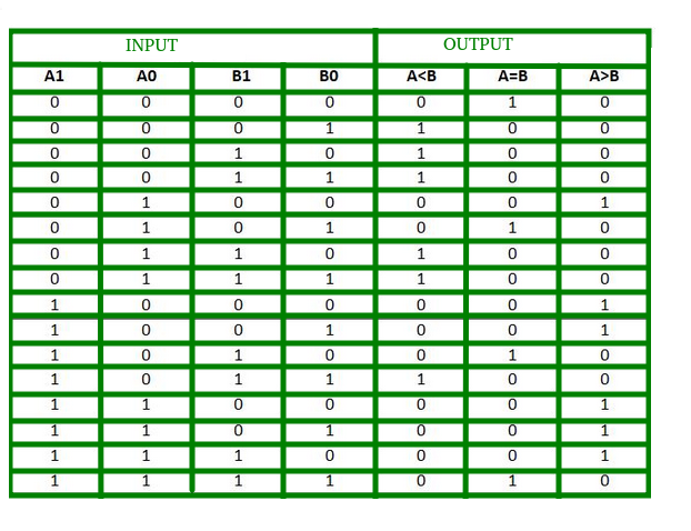
(a) Explain the 2-bit comparator circuit.
A 2-bit comparator circuit is a digital circuit that compares two 2-bit binary numbers and produces a signal indicating which number is greater, equal or less than the other. The comparator circuit typically has 2-bit inputs A and B, and several output signals indicating the comparison result.
Block Diagram:
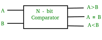
Truth Table:
(b) Write a short note on FPGA.
A Field-Programmable Gate Array (FPGA) is a type of programmable integrated circuit that allows for the implementation of digital logic circuits, such as combinational and sequential circuits, through the configuration of a set of programmable logic blocks and programmable interconnects. FPGAs are widely used in a variety of applications such as digital signal processing, embedded systems, and computer networking.
FPGAs consist of a large number of programmable logic elements (PLEs) and programmable interconnects (PICs) that can be configured to implement a wide range of digital logic circuits. The PLEs are typically made up of look-up tables (LUTs) and flip-flops, while the PICs allows for the routing of signals between the PLEs.
FPGAs are highly flexible and can be reprogrammed to implement different logic circuits, making them suitable for applications that require frequent changes or upgrades. They also offer a high level of parallelism, which can be useful for applications such as high-speed signal processing and image processing.
FPGAs are becoming increasingly popular in the field of embedded systems, as they offer a cost-effective and power-efficient alternative to traditional ASICs (Application-Specific Integrated Circuits) for low-volume and high-volume production.
(c) What is a Digital to Analog converter? Draw and Explain R-2R DAC.
A Digital-to-Analog Converter (DAC) is a type of circuit that converts a digital signal into an analog signal.
An R-2R ladder DAC is a type of digital-to-analog converter that uses a ladder of resistors to convert a digital signal into an analog signal. It is called R-2R because it uses two types of resistors, R and 2R.
The R-2R ladder DAC consists of a series of resistors connected in a ladder configuration. The most significant bit (MSB) of the digital input is connected to the top of the ladder, and the least significant bit (LSB) is connected to the bottom of the ladder. Each resistor in the ladder has a value of either R or 2R, depending on its position in the ladder.
The working of an R-2R ladder DAC can be described as follows:
- A digital word is applied to the inputs of the ladder.
- Depending on the value of each bit in the digital word, a current will flow through the corresponding resistor in the ladder.
- The current flowing through each resistor is proportional to the value of the corresponding bit in the digital word.
- The currents flowing through all the resistors are summed at the output, resulting in an analog voltage that is proportional to the digital input.
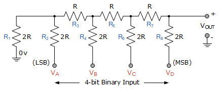
The R-2R ladder DAC is a popular choice for digital-to-analog conversion because it is relatively simple to construct and has good linearity and resolution. The circuit is simple since it uses only two types of resistors, and it has a high resolution since it uses a large number of resistors. The circuit is also relatively inexpensive, making it a cost-effective solution for many applications.
(a) Perform the following operation using 2’s complement method. (11010)2 – (1000)2
// Please provide the answer if you know
(b) Write a short note on Read Only Memory (ROM).
Read-Only Memory (ROM) is a type of non-volatile memory that stores data permanently and can only be read by a computer or other electronic device. It is called read-only because it can only be read from, not written to.
ROM is used in a wide range of electronic devices such as computers, cell phones, and other embedded systems. It is commonly used to store firmware, which is a set of instructions that control the basic functions of the device. The firmware is written to the ROM during the manufacturing process and cannot be changed or modified by the user.
There are several types of ROM, each with its own unique characteristics and uses. Some common types of ROM include:
- Mask ROM: which is programmed during the manufacturing process and cannot be reprogrammed afterward.
- Programmable ROM (PROM): which can be programmed once by the user, but cannot be reprogrammed afterward.
- Erasable Programmable ROM (EPROM): which can be reprogrammed by the user using ultraviolet light.
- Electrically Erasable Programmable ROM (EEPROM): which can be reprogrammed by the user using electrical signals.
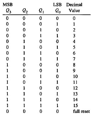
(c) Explain the working of a 4-bit binary ripple counter.
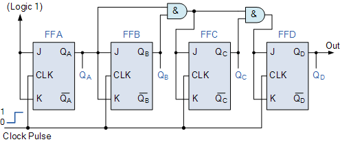
A 4-bit binary ripple counter is a type of counter that counts in binary and uses a ripple carry to increment the count. Here’s how it works step by step:
- The 4-bit binary ripple counter is made up of 4 flip-flops, each one representing a bit in the binary count. The first flip-flop is the least significant bit (LSB), and the fourth flip-flop is the most significant bit (MSB).
- Each flip-flop is connected to the clock input of the next flip-flop. When a clock pulse is applied, the first flip-flop changes state, and this change is propagated through the rest of the flip-flops.
- The output of each flip-flop is connected to the input of the next flip-flop, so that the output of the LSB flip-flop is connected to the input of the next flip-flop, the output of the next flip-flop is connected to the input of the next flip-flop, and so on. This causes the output of each flip-flop to change state when the previous flip-flop changes state.
- The 4-bit binary ripple counter will count from 0 to 15 in binary, incrementing the count by one each time a clock pulse is applied. The output of the counter represents the current count in binary.
For example, when the counter is at 0 (0000 in binary), the first clock pulse will cause the LSB flip-flop to change state, resulting in a count of 1 (0001 in binary).
The next clock pulse will cause the second flip-flop to change state, resulting in a count of 2 (0010 in binary). This process continues until the counter reaches 15 (1111 in binary), at which point the next clock pulse will cause the counter to overflow and reset back to 0 (0000 in binary).
OR
(a) Obtain the truth table of the function: F = xy+yz+zx.
| X | Y | Z | YZ | XY | XZ | XY+YZ+XZ |
| 0 | 0 | 0 | 0 | 0 | 0 | 0 |
| 0 | 0 | 1 | 0 | 0 | 0 | 0 |
| 0 | 1 | 0 | 0 | 0 | 0 | 0 |
| 0 | 1 | 1 | 1 | 0 | 0 | 1 |
| 1 | 0 | 0 | 0 | 0 | 0 | 0 |
| 1 | 0 | 1 | 0 | 0 | 1 | 1 |
| 1 | 1 | 0 | 0 | 1 | 0 | 1 |
| 1 | 1 | 1 | 1 | 1 | 1 | 1 |
(b) Implement the following functions using ROM. F1 = ∑m (1,3,4,6) and F2 = ∑m (0,1,5,7).
// Please provide the answer if you know
(c) Explain in detail the Dual Slope A/D converter.
A dual-slope A/D converter is a type of analog-to-digital (A/D) converter that uses a combination of two different conversion methods to achieve high resolution and accuracy.
The basic principle behind a dual-slope A/D converter is to measure the time required for an unknown input voltage to discharge a capacitor through a known resistor, and then convert that time into a digital value.
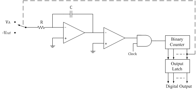
The dual-slope conversion process can be broken down into two main steps: the integration (or “ramping”) phase and the measurement (or “counting”) phase.
- Integration Phase: The input voltage is applied to the capacitor and the capacitor begins to charge. The capacitor is connected to a voltage comparator, which compares the input voltage to a reference voltage. When the input voltage equals the reference voltage, the comparator sends a signal to start the measurement phase.
- Measurement Phase: The input voltage is disconnected and a known constant current is applied to the capacitor through a known resistor. The capacitor begins to discharge, and the time it takes for the voltage on the capacitor to drop to a lower reference voltage is measured. This time is converted into a digital value using a timer circuit.
Conversion: The digital value obtained from the measurement phase is used to determine the input voltage.
The main advantage of dual-slope A/D converters is that they are very accurate and have high resolution. They are insensitive to the input voltage’s DC component, and the conversion process is not affected by noise or other disturbances.
However, the main disadvantage of dual-slope A/D converters is that they are relatively slow, taking a long time to convert an input voltage compared to other A/D converters.
Read More : DBMS GTU Paper Solution Winter 2021
Read More : DS GTU Paper Solution Winter 2021
“Do you have the answer to any of the questions provided on our website? If so, please let us know by providing the question number and your answer in the space provided below. We appreciate your contributions to helping other students succeed.